4. Important Points for PoP Techniques
The diagram below shows a collection of characteristic factors that affect the quality of PoP placement.
4-1.Defective Joining Due to Package Warp
The most important factor in the above diagram is package warp. The compatibility of the top package and bottom package is very important because the type of warp depends on the package. The package height must be controlled,especially because the bottom package is extremely thin. Since there are various types of package warp, it is important to know the warp characteristics of the top package,bottom package as well as the panel.
The above drawing shows examples of actual checks for warp behavior and compatibility between the top and bottom package. For the 12mm example,the top package warps upwards but the bottom package is warped upwards before reflow and changes to warp downwards while passing through reflow. for the 14mm example, the top package warps downwards but the bottom package is warped upwards before reflow.
Further to this the bottom package warps upwards at room temperature which is large change from the time it was warped downwards at the time of reflow.
Recently, it has become possible to control these warp trends to a certain degree at the package creation process. However, it is unavoidable that package warp changes occur due to heat, and people who use packages must recognize that the levelness of packages is different for room temperature and during reflow. The changes during reflow revert back to their original state at room temperature. However, it is important to be aware that the larger the part size, the easier the past size, the easier it is for the warp to be more significant during reflow.
The above pictures show examples of defecting joining. Look at the bottom package. It is easy to see that the shape of the joining area for the package center and edges is different.
Looking at an enlarged picture, the solder on the panel and bumps on the bottom of the package are not touching. A possible explanation is that the bottom packaged warped and was raised above the pads on the panel during the reflow process.
4-2.Transfer Amount
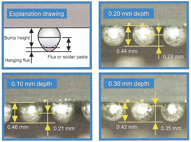
An adequate amount of solder must be transferred to join packages. If too much is used,shorting will occur. If too little is used, open defects will occur. The transfer amount depends on the dip depth during the dipping the dipping process. The dip depth is achieved using a mechanism that pushes the bumps down onto a transfer platform on a dip unit. This means that the transfer amount depends on the film thickness of the flux or solder paste. From experience, no problems will result of the thickness is set to be approximately half of the bump height. For example, the PoP top package has a bump pitch of 0.65 mm and bump diameter of 0.45 mm with a bump height of 0.40 mm. If the dip depth is set to 0.20mm, an adequate transfer amount can be achieved. As shown in the diagram below, a small cmount of flux has crept up the bump. However, after considering such things as the bump coplanarity, a setting of approximately 50 to 60% of the bump height should be used.

Other factors that influence the transfer amount besided the dip depth are the lowering speed, the raising speed and the length of time the part is held in the flux. All of these parameters can be specified. However, the transfer amount mostly depends on the dip depth and in testing, the other factors did not have such a large effct on the transfer amount. The raising speed had a small effect on the transfer rate but it was minor.
4-3. Flux Dipping
The pictures below show a side view of bumps with a height of 0.38 mm and flux applied. Each picture shows flux applied at a height of 0.10 mm, 0.20 mm and 0.30 mm. The line where flux is present is a little difficult to see. However, it was confirmed that flux crept up the bump further than the amount it was dipped in the flux (the flux film thickness). When the film thickness is 0.30 mm, there are cases in which the flux actually reaches the bottom of the package.
4-4.Solder Transfer
Other than transferring flux to bumps on the package, solder paste developed especially for PoP is used. This solder paste is a mix of solder with a particle diameter smaller than normal
(approx.10 u m) and flux. Normal solder paste does not have enough solder particles to sufficiently join the packages. However, the PoP solder paste ensures that a uniform thickness of solder coats the bumps, which is effective in preventing defective joining due to package warp. Although, if too much solder is applied, there is a greater chance that bridging will occur. Therefore, care should be taken not to supply an excessive amount of solder.

The pictures above show a side view of bumps with solder paste applied. The bump height is the same as before, 0.38 mm, and flux is applied at a height of 0.10 mm, 0.20 mm, 0.25 mm and 0.30 mm. Just as with flux, the solder paste also creeps up the bumps greater than the film thickness. In testing, a transfer amount of 0.20 mm was the best for bump heights of 0.38 mm.An approximate amount of 0.07 mm hanging solder paste was present on the bottom of the bump for this transfer amount. However, this hanging solder paste will help to join the top and bottom package together when a gap is created between the top package bumps and bottom package pads due to warping.
4-5.Self-alignment Effect in PoP
Generally, solder paste works more efficiently than flux for self-alignment.
4-6.Process Equipment Requirements
After considering each factor discussed so far, to ensure success in PoP placement, the following conditions for process equipment are required.
[Placement machine]
.High precision head - placement accuracy,Z-axis control
.Productivity - batch dipping with multiple nozzles
.Transfer check function - vision recognition
[Dip process]
.Film thickness adjustment
.Automatic flux supply
.simple operation, maintenance


